
Bio-Inspired Electronic Eyes and Synaptic Photodetectors for Mobile Artificial Vision
Abstract:
Conventional imaging and data processing devices are not ideal for mobile artificial vision applications, such as vision systems for drones and robots, because of the heavy and bulky multilens optics in the camera modules. Furthermore, the physically isolated image data processing units of conventional systems induce large power consumption and data latency. For mobile artificial vision applications, electronic eyes, including neuromorphic ones, have been developed inspired by biological eyes and neural networks. Here, we summarize the development of such bio-inspired electronic eyes and synaptic photodetectors (PDs). Bio-inspired electronic eyes, typically consisting of curved image sensor arrays, enable aberration-free imaging and module size miniaturization in addition to other advantageous optical features, such as wide field-of-view and deep depth-of-field. Furthermore, photodetecting devices with synaptic properties can efficiently enhance image contrast because of photon-triggered synaptic plasticity. Therefore, the signal-to-noise ratio of the acquired image can be enhanced, which facilitates efficient image recognition for machine vision. A brief summary of the remaining challenges and prospects concludes this review.
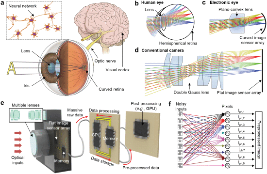
Artificial vision inspired by natural vision system and neural network. (a) Schematic of human vision and recognition system. The incident light is focused by the lens, detected and preprocessed by the curved retina, and recognized by the neural network in the visual cortex. Inset shows the neural network comprised of neurons and synapses. (b) Ray tracing simulation of human eye model. Reproduced with permission from [7]. Copyright 2020 Nature Publishing Group (NPG). (c) Ray tracing simulation of bio-inspired electronic eye consisting of a plano-convex lens and curved image sensor array. (d) Ray tracing simulation of conventional camera consisting of double Gauss lens and flat image sensor array. Reproduced with permission from [25]. Copyright 2020 NPG. (e) Schematic showing the image acquisition and in-sensor preprocessing performed using the synaptic PD array. (f) Optoelectronic machine vision processor for image filtering tasks [e.g., edge detection (right top) and image embossing (right bottom)] based on analog vector-matrix multiplications. Reproduced with permission from [6]. Copyright 2020 Wiley-VCH. (g) Schematic of an image sensor-based neural network. Inset shows a schematic of in-sensor pattern classification achieved by the image sensor-based neural network. Reproduced with permission from [37]. Copyright 2020 NPG.
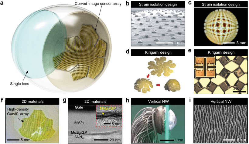
Cured image sensor arrays for bio-inspired electronic eyes. (a) Schematic of a bio-inspired electronic eye composed of a single lens and curved image sensor array. (b) Scanning electron microscopy (SEM) image of a curved image sensor array with a pop-up structure. Reproduced with permission from [41]. Copyright 2008 NPG. (c) Optical microscope image of a curved image sensor array with serpentine-shaped interconnections. Reproduced with permission from [44]. Copyright 2011 National Academy of Sciences (NAS). (d) Schematic showing that a silicon image sensor array with truncated icosahedron design deforms into a hemispherical format. Reproduced with a permission from [46]. Copyright 2017 NPG. (e) Optical microscope image of a shape-deformable PD array under biaxial stretching. The inset shows the undeformed device. Reproduced with permission from [47]. Copyright 2021 NPG. (f) Photograph of a high-density curved image sensor array based on 2-D materials and the truncated icosahedron design. (g) Transmission electron microscope image of an ultrathin image sensor array based on the MoS2/graphene heterostructure. Reproduced with permission from [11]. Copyright 2017 NPG. (h) Photograph of a hemispherical electrochemical eye with high-density perovskite nanowire array. (i) SEM image of vertically aligned perovskite nanowires. Reproduced with permission from [52]. Copyright 2020 NPG.
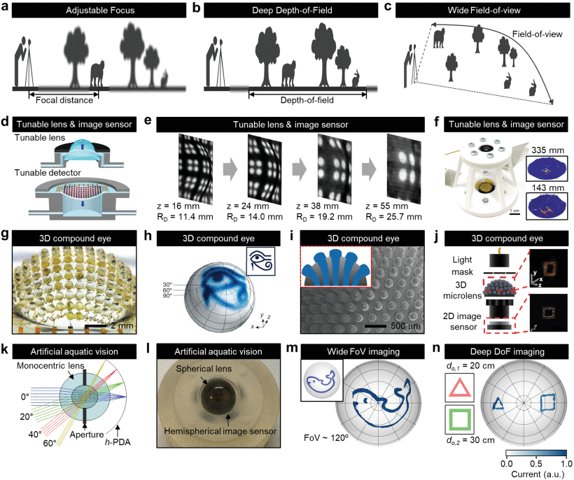
Electronic eyes for mobile artificial vision applications. Schematic of the optical properties required in mobile artificial vision applications, including (a) focus adjustment, (b) deep depth-of-field, and (c) wide field-of-view. (d) Schematic of focus-adjustable electronic eye with a tunable lens and deformable curved PD array. The shape of lens and PD array is tunable by a microfluidic system. (e) Images acquired by the focus-adjustable electronic eye under four conditions. The objects are located at different distances (z) , and the radii of curvature (RD) of the PD array are adjusted to match those of each focal plane. Reproduced with permission from [44]. Copyright 2011 NAS. (f) Photograph of focus-adjustable electronic eye consisting of an electrically tunable lens and a magnetically deformable curvy PD array. The inset shows the acquired images of the objects located at different distances. Reproduced with permission from [47]. Copyright 2021 NPG. (g) Photograph of an artificial compound eye exhibiting deep depth-of-field and wide field-of-view. (h) Wide field-of view image captured by the artificial compound eye. Reproduced with permission from [56]. Copyright 2013 NPG. (i) SEM image of a microlens array that optically connects omnidirectional incident light to a planar image sensor through waveguides. The inset shows the cross-sectional structure of the microlens array. (j) Imaging setup for capturing the images incident to the 3-D microlens array by optically guiding the light to the planar image sensor. Reproduced with permission from [55]. Copyright 2021 NPG. (k) Ray tracing simulation of aquatic vision-inspired electronic eye. Reproduced with permission from [7]. Copyright 2020 NPG. (l) Photograph of an aquatic vision-inspired electronic eye consisting of a spherical lens and a hemispherical image sensor array. Reproduced with permission from [16]. Copyright 2016 NPG. (m) Wide field-of-view and (n) deep depth-of-field imaging results obtained by the aquatic vision-inspired electronic eye. Reproduced with permission from [7]. Copyright 2020 NPG.
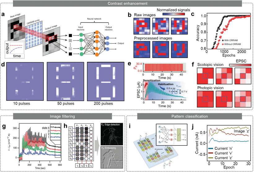
Synaptic PDs for in-sensor image processing. (a) Schematic showing in-sensor preprocessing performed by synaptic PDs to improve image recognition. The inset shows the time-dependent current output of the synaptic PDs compared with the instant current output of the conventional image sensor. (b) Preprocessed images with enhanced contrast compared to the noisy raw images. (c) Image recognition rate of the preprocessed images and noisy raw images at each training epoch. Reproduced with permission from [64]. Copyright 2019 NPG. (d) Images acquired during in-sensor preprocessing. The different numbers of optical pulses are irradiated to the synaptic PD. Reproduced with permission from [65]. Copyright 2021 NPG. (e) Schematic showing the habituation behavior of the sensory nervous system. (f) Preprocessed images acquired under scotopic (top) and photopic (bottom) conditions. Reproduced with permission from [67]. Copyright 2021 Wiley-VCH. (g) Photocurrent generation and decay characteristics for programming the conductance of four pixels of synaptic PD array. (h) Target kernels for image filtering (top) and the corresponding optically programmed kernels based on the conductance of crossbar array (bottom). Reproduced with permission from [6]. Copyright 2020 Wiley-VCH. (i) Microscope image of an image sensor integrated with neural networks. (j) Currents of the image sensor-based neural network in response to the illumination of noisy image of letter “z” during each training epoch. Reproduced with permission from [37]. Copyright 2020 NPG.
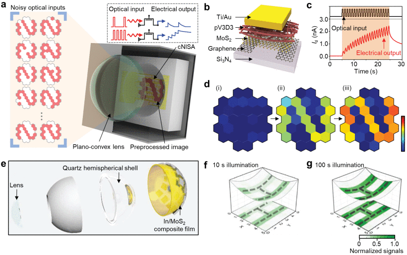
Neuromorphic-type electronic eyes based on curved synaptic PD arrays. (a) Schematic showing a neuromorphic-type electronic eye consisting of a plano-convex lens and cNISA. The neuromorphic-type electronic eye derives the preprocessed image from the noisy optical inputs through single lens-based image acquisition and in-sensor preprocessing. The inset shows the photon-triggered synaptic plasticity of the synaptic phototransistor. (b) Schematic of a synaptic phototransistor based on the MoS2-pV3D3 heterostructure. (c) Long-term potentiation of the synaptic phototransistor in response to frequent optical pulses. (d) In-sensor preprocessing for contrast enhancement performed by the neuromorphic-type electronic eye. Reproduced with permission from [25]. Copyright 2020 NPG. (e) Exploded schematic showing the neuromorphictype electronic eye consisting of a single lens and hemispherical synaptic PD array. The preprocessed images obtained after illuminating the pattern of letter “H” for (f) 10 s and (g) 100 s, respectively. Reproduced with permission from [72]. Copyright 2021 Wiley-VCH.
M. F. Amir, D. Kim, J. Kung, D. Lie, S. Yalamanchili and S. Mukhopadhyay, "NeuroSensor: A 3D image sensor with integrated neural accelerator," 2016 IEEE SOI-3D-Subthreshold Microelectronics Technology Unified Conference (S3S), Burlingame, CA, USA, 2016, pp. 1-2.
doi: 10.1109/S3S.2016.7804406
keywords: {Three-dimensional displays;Bandwidth;Random access memory;Memory management;Computational modeling;Feature extraction;Image sensors},
URL: http://ieeexplore.ieee.org/stamp/stamp.jsp?tp=&arnumber=7804406&isnumber=7804370
J. Abbott et al., "CMOS electronics probe inside a cellular network — Invited review paper," 2018 IEEE Custom Integrated Circuits Conference (CICC), San Diego, CA, USA, 2018, pp. 1-7.
doi: 10.1109/CICC.2018.8357046
keywords: {Electrodes;Integrated circuits;Parallel processing;Transistors;Bandwidth;Action potentials;Clamps;electrophysiology;neuroscience;cardiology;nano-bio interface;nanotechnology;nanoelectrode array;CMOS integrated circuit;intracellular recording},
URL: http://ieeexplore.ieee.org/stamp/stamp.jsp?tp=&arnumber=8357046&isnumber=8357004
S. Hong, S. Lee and D. Kim, "Materials and Design Strategies of Stretchable Electrodes for Electronic Skin and its Applications," in Proceedings of the IEEE, vol. 107, no. 10, pp. 2185-2197, Oct. 2019.
doi: 10.1109/JPROC.2019.2909666
keywords: {Electrodes;Skin;Nanomaterials;Substrates;Sensors;Fabrication;Human computer interaction;Electronic skin (e-skin);human–machine interface (HMI);integrated system;stretchable electrode;stretchable electronics},
URL: http://ieeexplore.ieee.org/stamp/stamp.jsp?tp=&arnumber=8695706&isnumber=8858047
S. Koyama, Y. Inaba, M. Kasano and T. Murata, "A Day and Night Vision MOS Imager With Robust Photonic-Crystal-Based RGB-and-IR," in IEEE Transactions on Electron Devices, vol. 55, no. 3, pp. 754-759, March 2008.
doi: 10.1109/TED.2007.914828
keywords: {Image color analysis;Cameras;Optical filters;Photonic crystals;Night vision;Silicon;Robustness;Color filter;day and night vision imager;image sensor;IR-cut filter;near-infrared;photonic crystal},
URL: http://ieeexplore.ieee.org/stamp/stamp.jsp?tp=&arnumber=4455782&isnumber=4455723
D. Chatterjee and A. Kottantharayil, "A CMOS Compatible Bulk FinFET-Based Ultra Low Energy Leaky Integrate and Fire Neuron for Spiking Neural Networks," in IEEE Electron Device Letters, vol. 40, no. 8, pp. 1301-1304, Aug. 2019.
doi: 10.1109/LED.2019.2924259
keywords: {Neurons;Biological neural networks;FinFETs;Integrated circuit modeling;Biological system modeling;Semiconductor process modeling;Bulk FinFET;impact ionization;leaky integrate and fire neuron;spiking neural network (SNN)},
URL: http://ieeexplore.ieee.org/stamp/stamp.jsp?tp=&arnumber=8743484&isnumber=8771270