
Electronic Waste Reduction through Devices and Printed Circuit Boards designed for Circularity
Abstract:
The development of Printed Circuit boards (PCBs) has so far followed a traditional linear economy value chain, leading to high volumes of waste production and loss of value at the end-of-life. Consequentially, the electronics industry requires a transition to more sustainable practices. This review article presents an overview of the potential solutions and new opportunities that may arise from the greater use of emerging sustainable materials and resource-efficient manufacturing. A brief contextual summary about how the international management of Waste PCBs (WPCBs) and legalization have evolved over the past 20 years is presented along with a review of the existing materials used in PCBs. The environmental and human health assessment of these materials relative to their usage with PCBs is also explained. This enables the identification of which eco-friendly materials and new technologies will be needed to improve the sustainability of the industry. Following this, a comprehensive analysis of existing WPCB processing is presented. Finally, a detailed review of potential solutions is provided, which has been partitioned by the use of emerging sustainable materials and resource-efficient manufacturing. It is hoped that this discussion will transform existing manufacturing facilities and inform policies, which currently focus on waste management towards waste reduction and zero waste.
Fig. 1. Circular electronics as a way forward to manage WPCB and eventually leading to zero waste
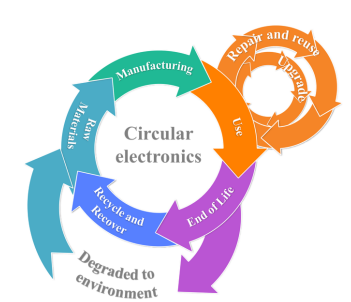
Fig. 2. (a) Global WEEE generated by year in Mt, (b) Application
owned per capita versus purchasing power parity, (c) E-waste and
e-waste/inhabitant vs. GDP per capita, reproduced with
permission from [41].
owned per capita versus purchasing power parity, (c) E-waste and
e-waste/inhabitant vs. GDP per capita, reproduced with
permission from [41].
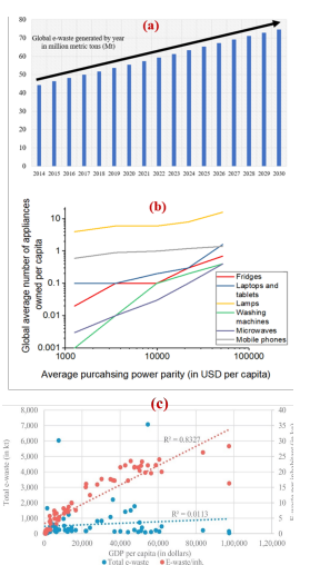
Fig. 3. Academic progress in tackling WEEE using a keyword
search from dimension app [42].
search from dimension app [42].
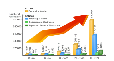
Fig. 4. Amount of waste PCBs from WEEE in the year 2021.
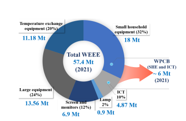
Fig. 5. Evolution of IC packaging and future directions
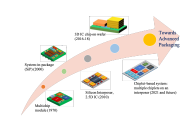
Fig. 6: (a) Relative abundance of materials in mobile phone (ppm),
(b) Global abundance of materials used in smartphone within the
earth crust or ocean (ppm), (c) Cost (€/kg) of materials used in
mobile phone.
(b) Global abundance of materials used in smartphone within the
earth crust or ocean (ppm), (c) Cost (€/kg) of materials used in
mobile phone.
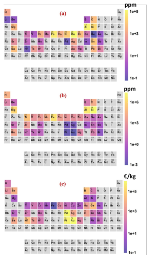
Fig. 7: Impact score of various PCB materials in terms of (a)
Ecotoxicity, and (b) Human Toxicity (grey means no information, or
no impact)
Ecotoxicity, and (b) Human Toxicity (grey means no information, or
no impact)
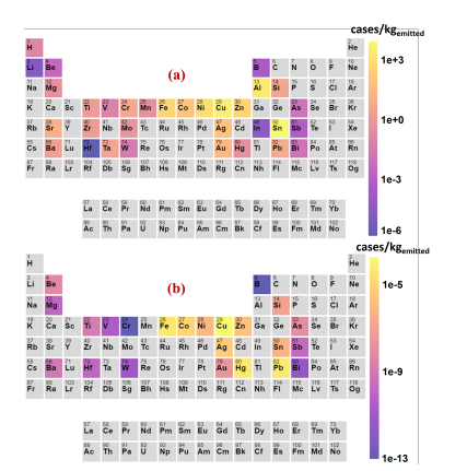
Fig. 8. Comparison of the CEENE analysis for the recycling and landfill scenario, reproduced with permission from [51]
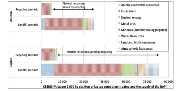
Fig. 9: General scheme for WPCB recycling.
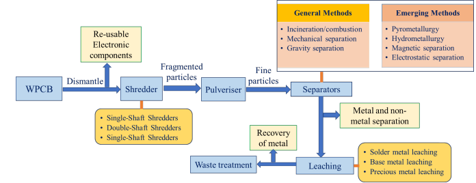
Fig. 10. Examples of biodegradable electronics
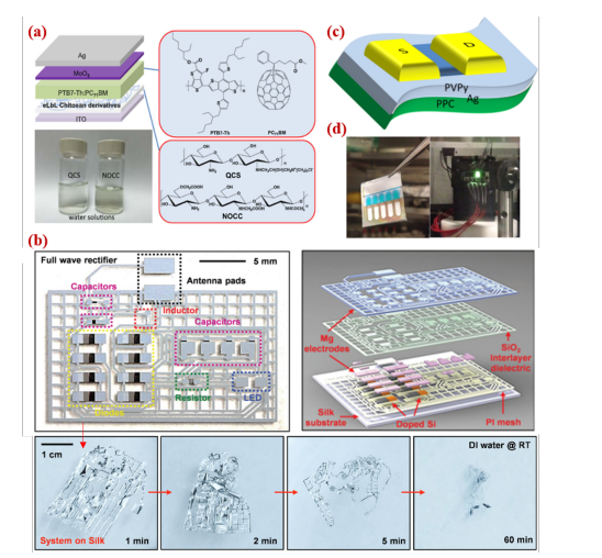
Fig. 11. Biodegradable energy harvesting devices.
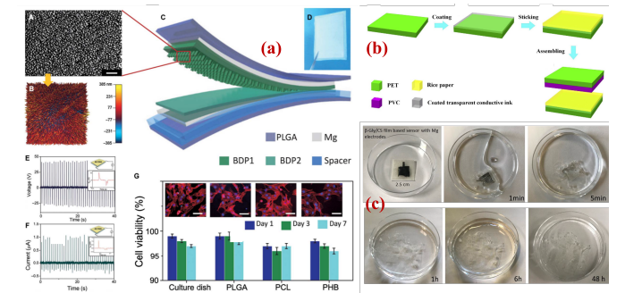
Fig. 12. Device and parts level sustainability of PCB
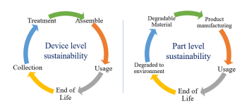
Fig. 13. Example of (a)-(b) three-stage neural network algorithm
based PCB sorting for efficient recycling, reproduced.
based PCB sorting for efficient recycling, reproduced.
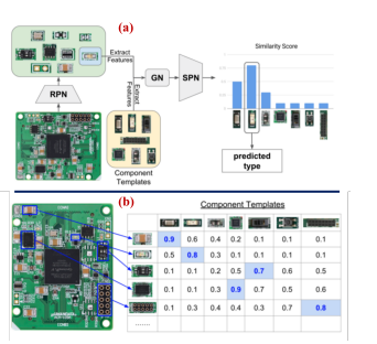
Fig. 14: Key design guidelines for recycling and reuse of PCBs.
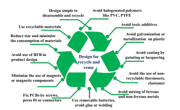
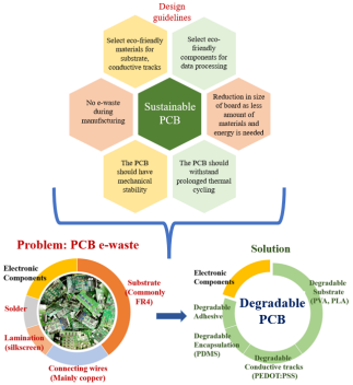
Fig. 15: Design guidelines of future degradable PCBs.
[1] H. Jun and M. Kim, "From Stakeholder Communication to Engagement for the Sustainable Development Goals (SDGs): A Case Study of LG Electronics," Sustainability, vol. 13, no. 15, p. 8624, 2021.
[2] U. N. C. o. Trade and Development, "Digital Economy Report 2019: Value creation and capture: implications for developing countries," ed: United Nations Publications New York, NY, 2019.
[3] U. S.-G. s. High-Level, "Panel on Digital Cooperation," The Age of Digital Interdependence Report, 2019.
[4] O. Ozioko and R. Dahiya, "Smart Tactile Gloves for Haptic Interaction, Communication, and Rehabilitation," Advanced Intelligent Systems, vol. 4, no. 2, p. 2100091, 2022.
[5] P. Escobedo, M. Bhattacharjee, F. Nikbakhtnasrabadi, and R. Dahiya, "Smart Bandage With Wireless Strain and Temperature Sensors and Batteryless NFC Tag," IEEE Internet of Things Journal, vol. 8, no. 6,
pp. 5093-5100, 2020.
[6] M. Chakraborty and K. Biswas, "Milk tester: Simultaneous detection of fat content and adulteration," IEEE Transactions on Instrumentation and Measurement, vol. 69, no. 5, pp. 2468-2476, 2020.
[7] M. Chakraborty and K. Biswas, "Hardware platform to detect fat percent in milk using a lipase immobilized PMMA-coated sensor," IEEE Transactions on Instrumentation and Measurement, vol. 68, no. 11, pp. 4526-4534, 2019.
[8] "Consumer Electronics - Worldwide. (n.d.). ." https://www.statista.com/outlook/dmo/ecommerce/electronicsmedia/consumer-electronics/worldwide (accessed October 18, 2021).
[9] A. K. Awasthi, J. Li, L. Koh, and O. A. Ogunseitan, "Circular economy and electronic waste," Nature Electronics, vol. 2, no. 3, pp. 86-89, 2019.
[10] C. Y. Yuan, H. C. Zhang, G. McKenna, C. Korzeniewski, and J. Li, "Experimental studies on cryogenic recycling of printed circuit board," The International Journal of Advanced Manufacturing Technology,
vol. 34, no. 7-8, pp. 657-666, 2007.
[11] X. Chen, J. Zhu, J. Ruan, Y.-t. Tang, and R.-l. Qiu, "Debromination and decomposition mechanisms of phenolic resin molecules in ball milling with nano-zerovalent iron," ACS Sustainable Chemistry & Engineering, vol. 8, no. 1, pp. 172-178, 2019.
[12] "A New Circular Vision for Electronics, Time for a Global Reboot."
https://www.unep.org/news-and-stories/press-release/un-report-time-seize-opportunity-tackle-challenge-e-waste (accessed Novembe 11,2021).